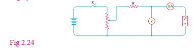
- Volt-ampere or V-I characteristic of a pn junction (also called a crystal or semiconductor diode) is the curve between voltage across the junction and the circuit current. Usually, voltage is taken along x axis and current along y-axis. Fig. 2.24 shows the *circuit arrangement for determining the V-I characteristics of a pn junction. The characteristics can be studied under three heads, namely; zero external voltage, forward bias and reverse bias.
 (i) Zero external voltage:
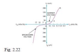
 When the external voltage is zero, i.e. circuit is open at K, the potential barrier at the junction does not permit current flow. Therefore, the circuit current is zero as indicated by point O in Fig. 2.22.
 (ii) Forward bias:
 With forward bias to the pn junction i.e. p-type connected to positive terminal and n- type connected to negative terminal, the potential barrier is reduced. At some forward voltage (0.7 V for Si and 0.3 V for Ge), the potential barrier is altogether eliminated and current starts flowing in the circuit. From now onward, the current increases with the increase in forward voltage. Thus, a rising curve OB is obtained with forward bias as shown in Fig. 2.22. From the forward characteristic, it is seen that at first (region OA), the current increases very slowly and the curve is non-linear. It is because the external applied voltage is used up in overcoming the potential barrier. However, once the external voltage exceeds the potential barrier voltage, the pn junction behaves like an ordinary conductor.
- Therefore, the current rises very sharply with increase in external voltage (region AB on the curve). The curve is almost linear.
(iii)Reverse bias: With reverse bias to the pn junction i.e. p-type connected to negative terminal and n- type connected to positive terminal, potential barrier at the junction is increased. Therefore, the junction resistance becomes very high and practically no current flows through the circuit.
However, in practice, a very small current (of the order of µA) flows in the circuit with reverse bias as shown in the reverse characteristic. This is called reverse saturation current (I
s) and is due to the minority carriers. It may be recalled that there are a few free electrons in p-type material and a few holes in n-type material. These undesirable free electrons in p-type and holes in n-type are called minority carriers.
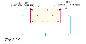
- As shown in Fig. 2.26, to these minority carriers, the applied reverse bias appears as forward bias. Therefore, a small current flows in the reverse direction.
- If reverse voltage is increased continuously, the kinetic energy of electrons (minority carriers) may become high enough to knock out electrons from the semiconductor atoms. At this stage breakdown of the junction occurs, characterized by a sudden rise of reverse current and a sudden fall of the resistance of barrier region. This may destroy the junction permanently.
Note: The forward current through a pn junction is due to the majority carriers produced by the impurity.
- However, reverse current is due to the minority carriers produced due to breaking of some covalent bonds at room temperature.
Wilfykil answered the question on
August 14, 2019 at 05:53