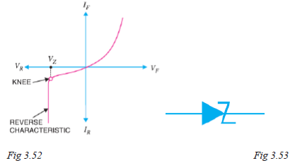
- It has already been discussed that when the reverse bias on a crystal diode is increased, a critical voltage, called breakdown voltage is reached where the reverse current increases sharply to a high value. The breakdown region is the knee of the reverse characteristic as shown in Fig. 3.52. The satisfactory explanation of this breakdown of the junction was first given by the American scientist C. Zener.
Therefore, the breakdown voltage is sometimes called Zener voltage and the sudden increase in current is known as Zener current.
- The breakdown or Zener voltage depends upon the amount of doping. If the diode is heavily doped, depletion layer will be thin and consequently the breakdown of the junction will occur at a lower reverse voltage. On the other hand, a lightly doped diode has a higher breakdown voltage.
- When an ordinary crystal diode is properly doped so that it has a sharp breakdown voltage, it is called a Zener diode.
- A properly doped crystal diode which has a sharp breakdown voltage is known as a Zener diode.
- Fig. 3.53 shows the symbol of a Zener diode. It may be seen that it is just like an ordinary diode except that the bar is turned into z-shape.

- The following points may be noted about the Zener diode:
(i) A Zener diode is like an ordinary diode except that it is properly doped so as to have a sharp breakdown voltage.
(ii) A Zener diode is always reverse connected i.e. it is always reverse biased.
(iii) A Zener diode has sharp breakdown voltage, called Zener voltage V
Z.
(iv) When forward biased, its characteristics are just those of ordinary diode.
(v) The Zener diode is not immediately burnt just because it has entered the breakdown region. As long as the external circuit connected to the diode limits the diode current to less than burn out value, the diode will not burn out.
Wilfykil answered the question on
August 14, 2019 at 09:24