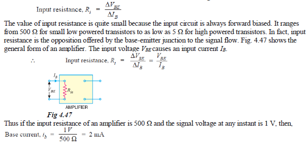
(i) Input resistance: It is the ratio of small change in base-emitter voltage (change in V
BE) to the resulting change in base current (change in I
B) at constant collector-emitter voltage i.e.
 (ii) Output resistance:
 It is the ratio of change in collector emitter voltage (change in V
CE) to the resulting change in collector current (change in I
C) at constant base current i.e.

- The output characteristics reveal that collector current changes very slightly with the change in collector- emitter voltage. Therefore, output resistance of a transistor amplifier is very high– of the order of several hundred kilo-ohms.
- The physical explanation of high output resistance is that collector-base junction is reverse biased.
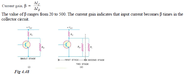
(iii) Effective collector load: It is the total load as seen by the a.c. collector current.
In case of single stage amplifiers, the effective collector load is a parallel combination of RC and RO as shown in Fig. 4.48 (i).
 (iv) Current gain:
 It is the ratio of change in collector current (change in I
C) to the change in base current (change in I
B)
i.e.
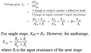
 (v) Voltage gain:
 It is the ratio of change in output voltage (change in V
CE) to the change in input voltage (?V
BE)
i.e.
 (vi) Power gain:
 It is the ratio of output signal power to the input signal power i.e.

Wilfykil answered the question on
August 15, 2019 at 07:51